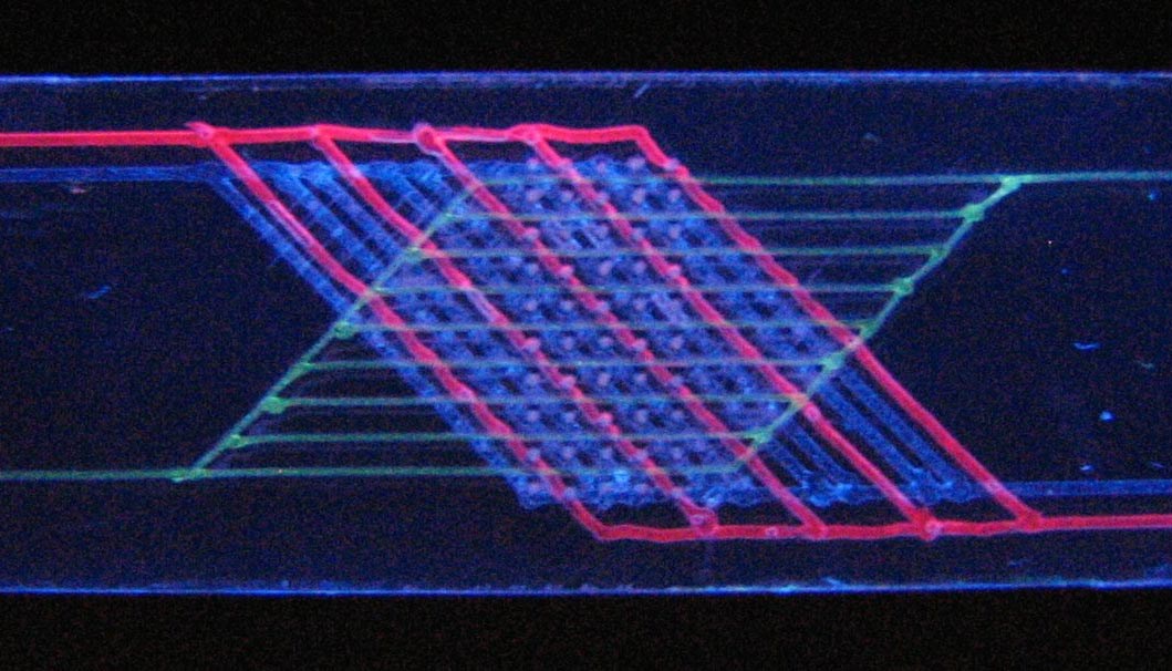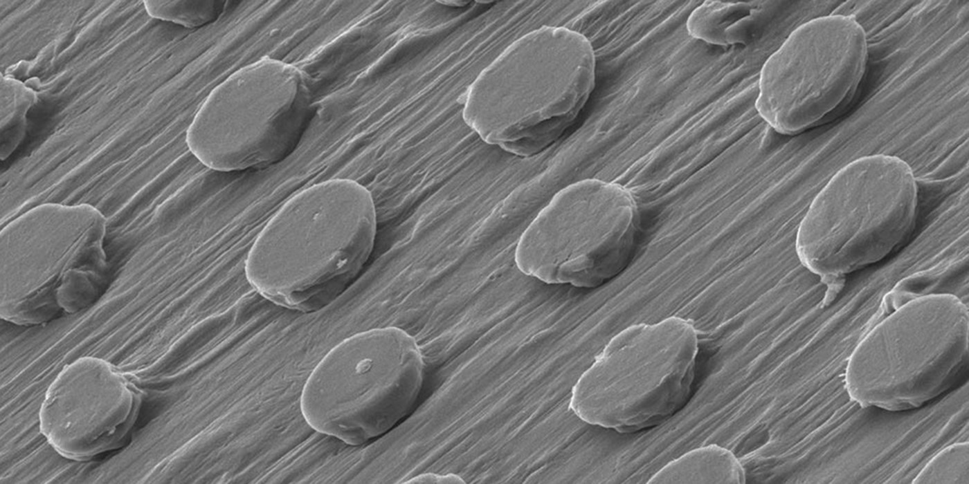
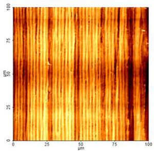
The UMass Lowell Center for Advanced Manufacturing of Polymers and Soft Materials (AMPS), formerly the Nanomanufacturing Center, leverages a strong plastics heritage along with industrial scale equipment to develop advanced nanomanufacturing processes, in a safe, reproducible and controlled environment.
Advancing Your Manufacturing Process
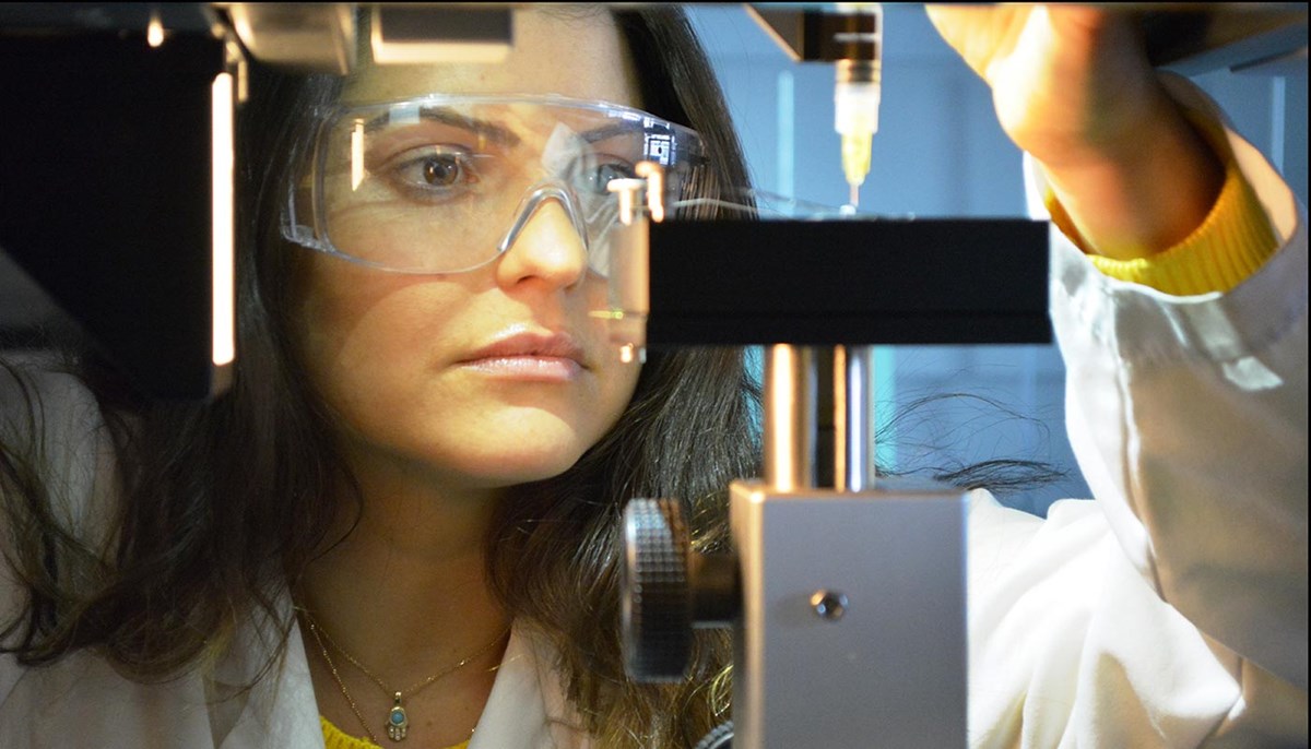
Why Collaborate with UMass Lowell?
National Leader in Advanced Polymer Processing
Unique Tools for Industry